Huawei unveils its LogicFolding architecture to bypass EUV lithography limits and target 1.4nm-equivalent chips by 2031
LogicFolding Kirin smartphone chips will ship this year.

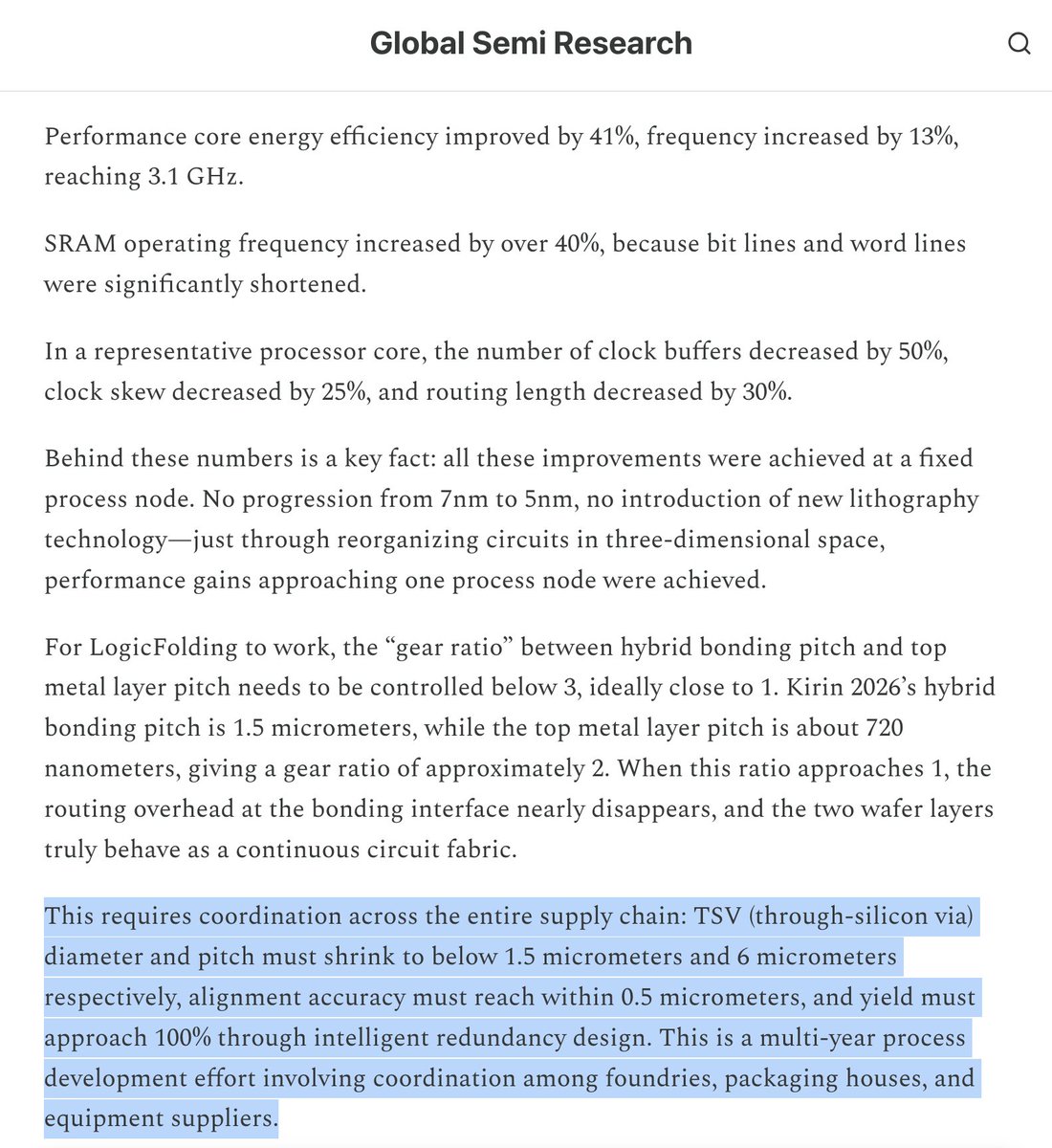
the dissidents are rattled; lashing out. No, obviously everyone will be doing advanced stacking, and was going to do it already. But now it is possible for Huawei to do better than previously expected.
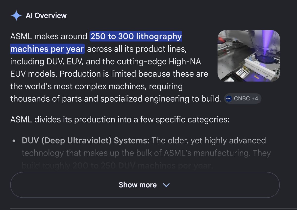
The Netherlands, pop. 18.4 million Taiwan, pop. 23.3 million China, pop. 1400 million I think we don't know how far DUV can go. The entire global semiconductor supply chain is BOUTIQUE, nobody has tried just spamming machines. ASML ships, what, 300 units per year? 1/2 Boeing?
 Zephyr@zephyr_z9
Now it all comes down to how fast they can scale DUV and expand capacity
 #517Andrew Curran@ANDREWCURRAN_
 Zephyr@zephyr_z9
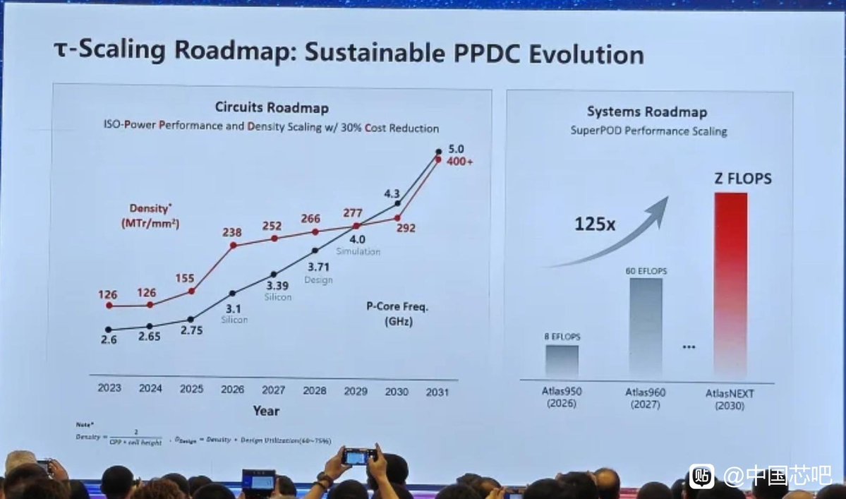
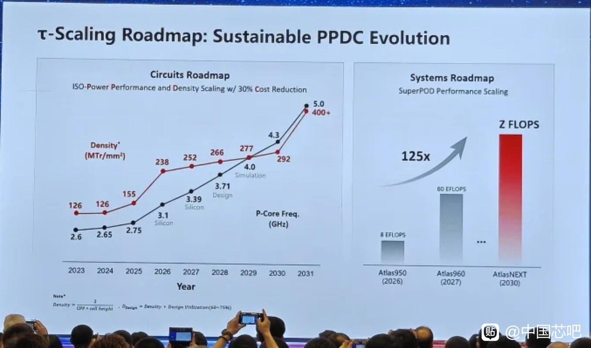
Very impressive roadmap 2026 will be a big density jump for them and good enough for most advanced AI chips
 #1496Chubby♨️@KIMMONISMUS
Chinas Huawei can't access EUV. So they wrote their own scaling law. The leverage of US export controls erodes.
Huawei just presented the Tau (τ) Scaling Law at IEEE ISCAS, a framework that replaces geometric transistor scaling with time-based optimization across devices, circuits, chips, and systems.
Huawei is not trying to win the nanometer race anymore. They're redefining it.
381 chips designed and mass-produced over six years. Kirin chips with their new LogicFolding architecture ship this fall. Target by 2031: transistor density equivalent to 1.4nm processes - without EUV (ASML embargo still hits hard)
Whether Tau Scaling delivers on that promise remains to be seen. But it shows one thing: US export controls cut Huawei off from cutting-edge lithography, and instead of hitting a wall, they built a parallel road.
China's semiconductor independence isn't hypothetical anymore. It's shipping in phones, running AI workloads, and now has its own scaling law presented at one of the world's top circuit design conferences.
If Huawei can close the performance gap through architecture instead of lithography, the entire leverage of US export controls erodes. The sanctions were designed to keep China two generations behind. Huawei is trying to make that metric irrelevant.
h/t @AndrewCurran_ for finding this interesting blogarticle and @zephyr_z9 for the photo
 Andrew Curran@AndrewCurran_
Huawei says it has made a breakthrough and expects to design high-end chips with transistor density equivalent to 1.4 nm processes by 2031.
#1497Zephyr@ZEPHYR_Z9Now it all comes down to how fast they can scale DUV and expand capacity
Zephyr@zephyr_z9Very impressive roadmap 2026 will be a big density jump for them and good enough for most advanced AI chips
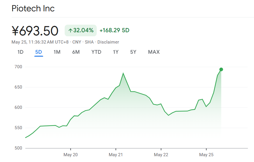
#1497Zephyr@ZEPHYR_Z9Btw, this is super bullish for hybrid bonding equipment suppliers, CMP suppliers (pads, slurry, equipment), & backside grinding equipment suppliers)
 Zephyr@zephyr_z9
Very impressive roadmap 2026 will be a big density jump for them and good enough for most advanced AI chips
 #1598Carlos E. Perez@INTUITMACHINE
Any experts want to chime in on the impact of this development on China's AI efforts?
 Huawei@Huawei
HUAWEI has presented the Tau (τ) Scaling Law, a new principle for guiding the future development of the semiconductor industry. By 2031, HUAWEI's high-end chips based on this law are expected to feature a transistor density that is equivalent to 14 Å (1.4 nm) processes.